Packaging technology development history
The development of packaging technology needs to meet the requirements of miniaturization, lightweight and high performance of electronic products. Therefore, packaging continues to evolve towards the goal of miniaturization, multi-pin and high integration.
Packaging can be classified in a variety of ways:
1) According to the material can be divided into: metal packaging, ceramic packaging, plastic packaging, etc.;
2) According to the connection with PCB board, it can be divided into PTH packaging and SMT packaging;
3) According to the package type, it can be divided into: SOT, SOIC, TSSOP, QFN, QFP, BGA, CSP, etc.

At present, the packaging technology is divided into traditional packaging and advanced packaging according to the packaging technology (welding line or not). The basic connectivity system of traditional packaging mainly uses lead bonding technology, while advanced packaging refers to various encapsulation methods that are mainly Bumping electrical connections, aiming at achieving more I/O and more integration functions.
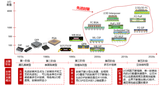
▲ Source: asset information network thousand international investment bank Yole
The historical development of packaging can be divided into five stages. Currently, the mainstream technologies in the global packaging industry are in the third stage, dominated by CSP and BGA, and the fourth and fifth stage encapsulation technologies represented by system-level packaging (SiP), reverse welding packaging (FC) and Bumping on chips.
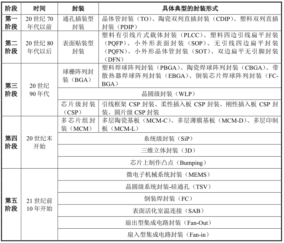
▲ Source: asset information network thousand international investment bank Yole
There is no absolute difference between the advantages and disadvantages of traditional packaging and the substitution relationship between advanced packaging. The increasing demand for high computing power and integration of downstream applications makes advanced packaging technology become the future development trend.
02
Advanced packaging form development
The development trend of advanced packaging technology can be decomposed into three sub-vectors:
(1) Functional diversification: the packaged object develops from the initial single nude to multiple nude, and there may be a variety of nude pieces with different functions under one package;
(2) Diversified connectivity: Encapsulation internal interconnection technologies are constantly diversified, with increasing connectivity density from Bumping to embedded interconnection;
(3) Stack diversification: device arrangement has gradually moved from plane to three-dimensional, and a rich stack topology is constructed by combining different interconnection modes. The development of advanced packaging technology extends and expands the concept of packaging, from wafers to systems can be used to describe integrated processing processes.
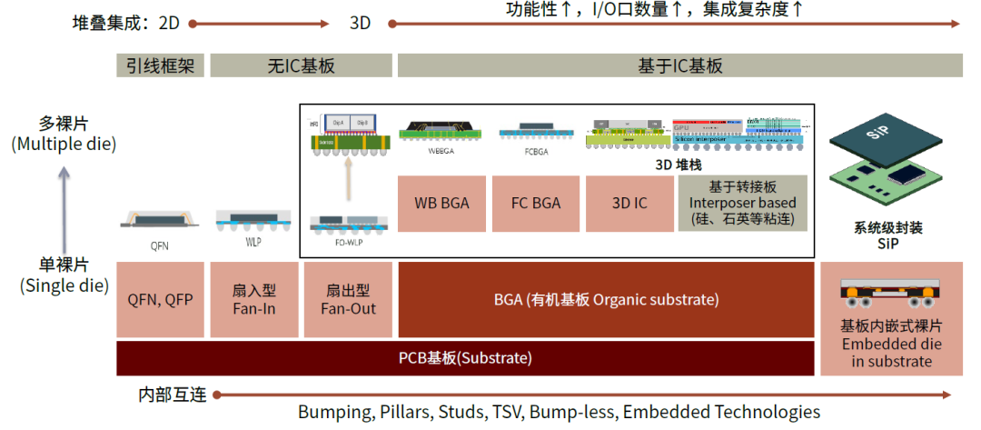
▲ Source: asset information network thousand international investment bank Yole
Semiconductor products are developing from 2D to 3D. From the direction of technology development, new packaging methods such as system level packaging (SiP) have appeared in semiconductor products, and from the technology implementation methods, such as flip, convex, wafer level packaging, 2.5D packaging, 3D packaging (TSV) and other advanced packaging technologies have appeared.
Mainstream advanced packaging forms are introduced
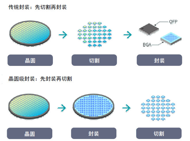
▲ Source: SK Hynix, Research Department of China International Capital Corporation
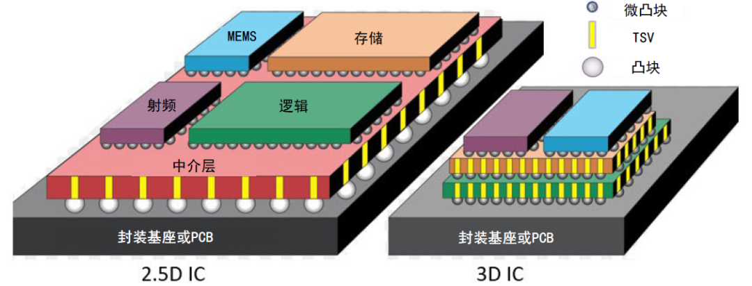
3D IC (Stereoscopic package)
Early versions of 3D ics rely on traditional interconnect methods (bonding/flip) for vertical stacking at the package level. Unlike 2.5D, 3D usually consists of stacked chips or devices.
▲ Source: Semiconductor Engineering, Research Department, China International Capital Corporation
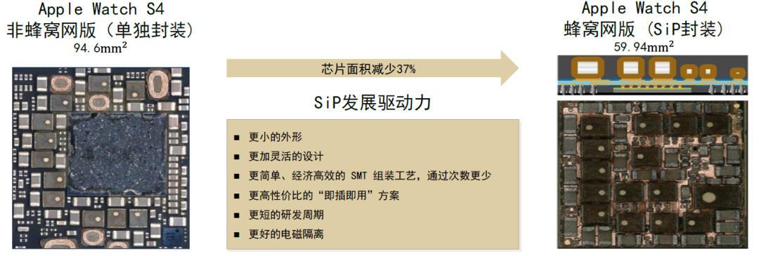
SiP (System level Encapsulation)
SiP is a system or subsystem composed of multiple active electronic components (usually bare chips), passive devices, and other devices (MEMS or optical devices, etc.) with different functions. Then, multiple systems are assembled into a package body to make it become a single package that can realize certain functions. From the connection mode, flip, fan out and Embedded Die are three common technical routes to implement SiP.
▲ Source: Semiconductor Engineering, Research Department, China International Capital Corporation
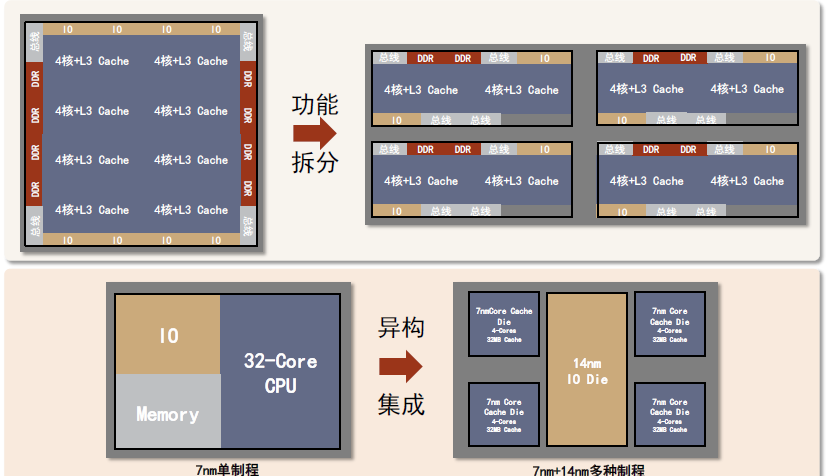
Chiplet(core)
Chiplet divides each function area of a single SOC chip into multiple independent chips, which are then encapsulated into a complete system.
▲ Source: AMD official website, research department of China International Capital Corporation
03
Development trend and competition pattern of advanced packaging
1, integrated circuit into the "post-moore era", advanced packaging prominent role
It is difficult to break through the process technology in the "post-Moore era", and the process is slowed down by the rising cost and technical barriers. As the IC process is difficult to break through in the short term, improving the overall performance of the chip through advanced packaging technology has become the development trend of the IC industry.
2. Advanced packaging will become the main growth point of the future closed test market
After the chip process technology has entered the "post-Moore era", advanced packaging has been widely used in high-end logic chips, memory, radio frequency chips, image processing chips, touch chips and other fields.
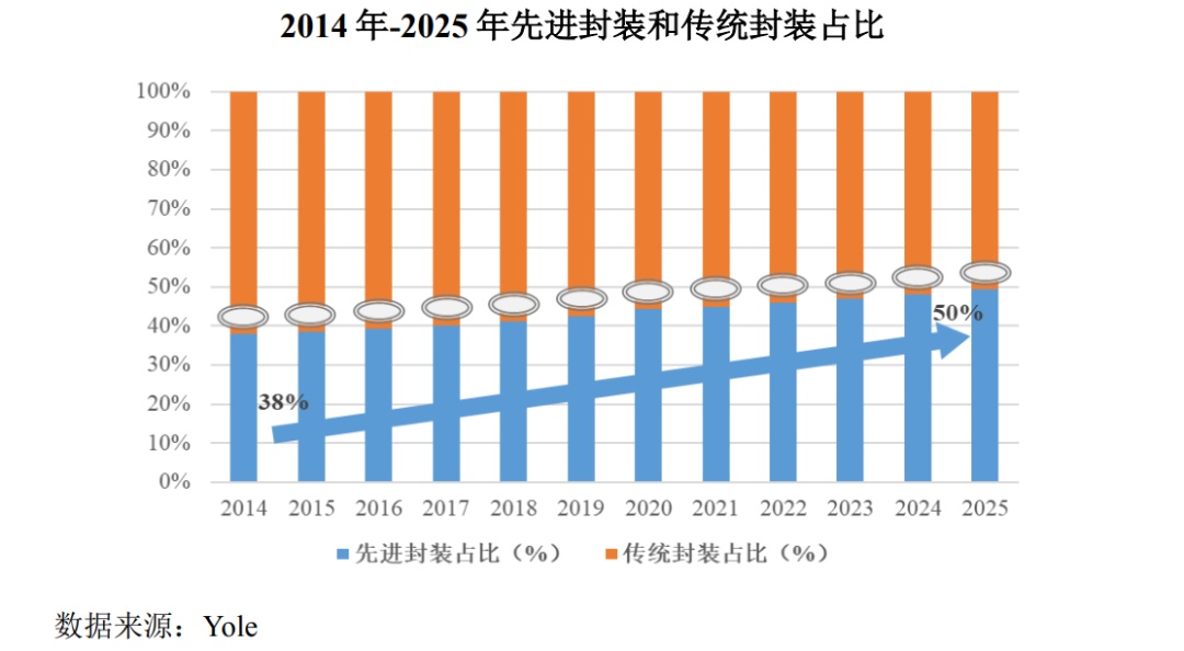
According to market research agency Yole forecast data, the global advanced packaging in the integrated circuit closed test market share will continue to increase. Yole, meanwhile, predicts that traditional packaging will grow at a compound annual growth rate of just 1.9% globally between 2019 and 2025, much slower than advanced packaging.
▲ Photo source: Yole
3. System Level Packaging (SiP) is an important driver for the growth of the advanced packaging market
System level packaging products are flexible, and the development cost and cycle time is much lower than that of a single chip system (SoC) with the same level of complexity.
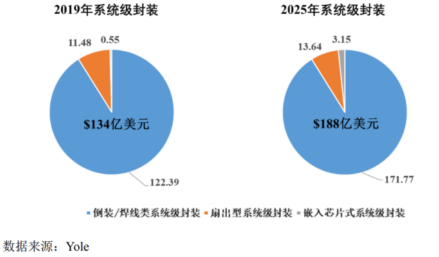
According to the statistics of Yole, the market research agency, in 2019, the global system-level packaging scale was 13.4 billion dollars, accounting for 23.76% of the world's entire closed test market share, and predicted that by 2025, the global system-level packaging scale will reach 18.8 billion dollars, with an annual compound growth rate of 5.81%.
▲ Photo source: Yole
In the system level packaging market, flip/solder wire system level packaging products account for the highest proportion. In 2019, flip/solder wire system level packaging products market size was $12.239 billion, accounting for 91.05% of the whole system level packaging market. According to Yole forecast data, in 2025 flip/wire type system level packaging will remain the mainstream system level packaging products, the market size will grow to 17.177 billion dollars.
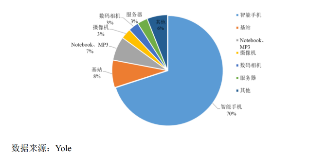
According to Yole, the fastest growing application markets for system-level packaging over the next five years will be wearables, Wi-Fi routers, IoT facilities, and telecommunications infrastructure.
▲ Photo source: Yole
4. High density and fine spacing convex flip products (FC) have a large development space in the mobile and consumer market
Advanced packaging revenue is expected to grow at a compound annual growth rate of 7.9% between 2020 and 2026, according to Yole. By 2026, the FC-CSP (flip chip size package) segment will reach more than $10 billion.
Broken down by revenue, the mobile and consumer markets accounted for 85% of total advanced packaging revenue in 2019, and Yole expects a compound annual growth rate of 5.5% to 2025, accounting for 80% of total advanced packaging revenue. While FC CSP packaging has a presence in the mobile and consumer markets, mainly for smartphone APUs, RF components and DRAM devices used in PC, server and automotive applications.
5. The flat pin-less package (QFN/DFN) product still has a large volume market
The QFN/DFN format is DFN, but its larger market volume makes it less likely to be replaced in the short term. The QFN/DFN class has the following advantages:
(1) Physical level: small size, light weight, high efficiency.
(2) Quality level: strong heat dissipation performance, good electrical performance, strong reliability.
(3) with higher cost performance

With the transformation and upgrading of the integrated circuit industry, policy and financial support, the rapid rise of the consumer electronics industry has promoted the development of the advanced packaging market, attracting the world's major mainstream IC packaging manufacturers in the field of advanced packaging for continuous layout.
1. Competition pattern of global integrated circuit packaging market: ASE and Samsung Electronics compete for power
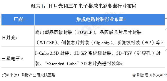
In the field of integrated circuit packaging, ASE and Samsung Electronics are the world leaders. Ase is one of the first companies to mass-produce SiP packages, and many wearable chip solutions choose ASE's SiP service. Ase also offers a full range of semiconductor testing services, including front-end engineering testing, wafer detection, logic/mixed signal/RF /(2.5D / 3D) modules, final testing of SiP/MEMS, and other test-related services. As an old integrated circuit giant, Samsung Electronics has the whole industrial chain layout from design, manufacturing to packaging, and its research and development direction is mainly advanced packaging.
Map Source: Qianzhan Industrial Research Institute
2. Competition pattern of China's IC packaging industry: it can be divided into three competitive echelons
The integrated circuit package market is concentrated and the competition is fierce. At present, the main participants in China's LCD packaging market are Changdian Technology, Tongfu micro Electronics, Huatian Technology and other enterprises, located in the first tier of competition are Changdian Technology, Tongfu micro electronics, Huatian Technology, three of the world's top ten closed test manufacturers in 2020; The second echelon has Jingfang Technology, Taiji Industry and other enterprises, the scale of which is different from the first echelon; Other mid - and low-end packaging manufacturers are in the third tier of competition.
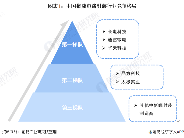
Map Source: Qianzhan Industrial Research Institute
From the regional distribution of IC packaging industry chain enterprises, IC packaging industry enterprises are mainly distributed in Jiangsu, Zhejiang, Shanghai and other coastal provinces and cities, among which Jiangsu Province has the largest number of IC sealing test enterprises. At the same time, the distribution of inland provinces is relatively dispersed, mainly concentrated in Gansu and Hunan.
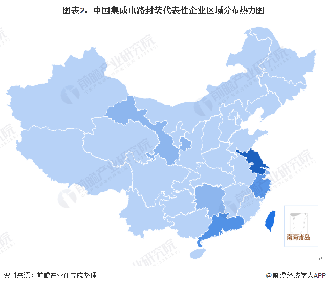
Map Source: Qianzhan Industrial Research Institute
From the distribution of representative enterprises, Jiangsu Changdian Technology Co., LTD., Tongfu Microelectronics Co., LTD., Suzhou Jingfang Semiconductor Technology Co., LTD.; Gansu as the center of the Tianshui Huatian Technology Co., LTD. High visibility.
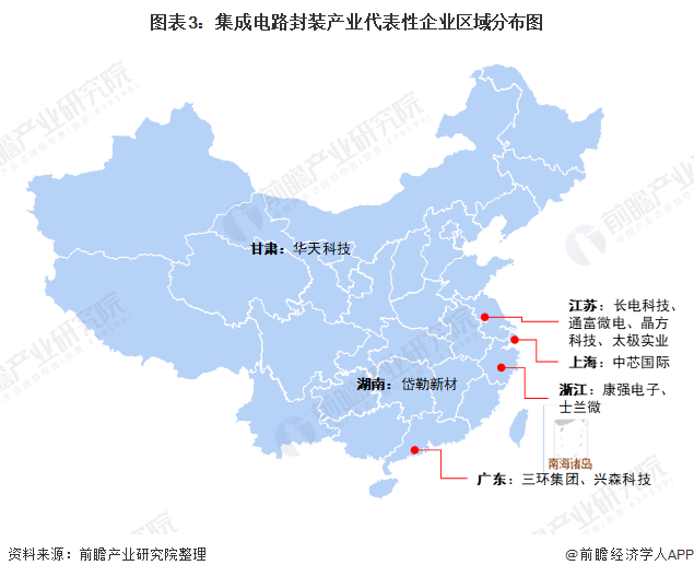 、
、
04
Advanced packaging equipment to domestic production
Taking advantage of the development of advanced packaging, advanced packaging equipment is gradually moving towards localization, and the domestic packaging equipment market is developing further.
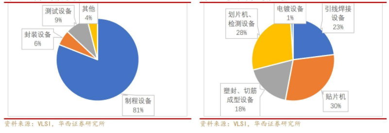
Closed test equipment can be divided into packaging equipment and test equipment two categories. In terms of packaging equipment, corresponding to the six processes of backside thinning wafer cutting, laminating, lead bonding, molding, molding and molding in lead bonding process, traditional packaging equipment is mainly divided into thinning machine, cutting machine, laminating machine, lead bonding machine, plastic sealing machine and rib cutting machine according to the process flow.
In the advanced packaging process that substitutes Bumping for lead bonding, equipment such as inverse machines, ball planting machines and reflux furnaces are also used, and photoliths, etching machines, electroplating machines, PVD, CVD and other semiconductor manufacturing bumping equipment are also used in advanced packaging processes.
Testing process is throughout the whole process of semiconductor manufacturing, which is mainly divided into design verification Test, process control test, CP, Circuit Probing and finished product test (FT, Final Test). CP test and FT test occur after wafer manufacturing and belong to semiconductor manufacturing post-test. The main test equipment for the test machine, probe table, sorting machine. CF test mainly uses test machine, probe machine; FT test mainly uses testing machine, sorting machine.
Process control testing is the testing of the whole process of wafer manufacturing, mainly using optical microscopes, defect observation equipment, etc. Design verification testing Due to the whole process of testing the chip sample, all the above-mentioned semiconductor testing equipment is required.

▲ Photo source: Huatai Research
Organization analysis pointed out that the development of advanced packaging will increase the demand for equipment: (1) packaging equipment needs to increase, such as grinding equipment (wafer need to make thinner), cutting equipment needs to increase, solidification equipment (DieBond requirements are higher); ② New equipment requirements: for example, bump process involves exposure, reflow welding and other equipment.

The global packaging equipment presents the oligopoly pattern, ASM Pacific, K&S, Besi, Disco, Towa, Yamada and other companies occupy the majority of the packaging equipment market, the industry local alternative space is large.
Tensun focuses on high-end precision equipment, mastering core technologies such as precision dispensing, precision slicing and precision operation control platform in depth; To the world - class quality standards, obtained a number of industry qualifications, patents and honors. Tensun Tensheng always adhere to technological innovation, dispensing equipment has become the main market selection, this year Jig Saw automatic sorting all-in-one machine formal volume output, further promote the advanced packaging market shipments, promote the semiconductor sealing equipment localization process!
The above content is from the Semiconductor Packaging Engineer's Home
Author: Zhao Gong


 、
、
